As I’ve been busy with real life ™, its been a while since I took a trip to the computer mall to see what new goodies I could play with.
A friend is in town from Beijing, so took him down to the Shanzhai hell (or heaven depending on PoV) that is Qiu Jiang lu.
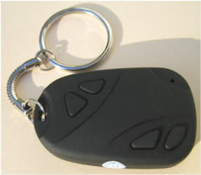
I wasn’t aware that you could buy Keychain video recorders for 80rmb, but you can. Apparently they’re even cheaper in eBay – although I don’t see how its possible, given that the factories here are pricing higher than they sell for in the States. Rejects?
Anyhow, I bought 2 keychain video camera’s, and an MP3 looking one.
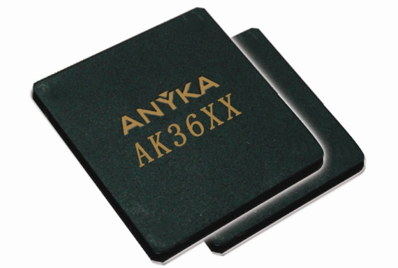
Dissected one and it contains the Anyka AK3651B as the main chip.
The AK36xx series is an SoC (System on a Chip).
As Anyka appears to be deathly afraid of giving out any useful information about their products, I’ve had to piece together info from what I found online.
Their own product page here – http://www.anyka.com/enProShow.asp?sortFlag=110&sortName=Application%20Processor&id=105
says the following:
32-bit Microprocessor Core
Integrated I/D cache
Memory Management Unit (MMU)Video Coprocessor
MPEG4.SP codec
H.263 codec
Motion JPEG codecAudio Coprocessor
MP3 decoder
WMA decoder
AAC/AAC+ decoder
AMR codec
Real-time audio stream in PCM/ADPCM formatImage Coprocessor
JPEG HW codecGlueless Dual LCD Displays
Supporting MPU LCD
Supporting RGB LCD
Programmable LCD size and refreshing rateConnectivity
USB 2.0 HS OTG
I2S master/slave
UART
SPI
MMC/SDEmbedded ADCs and DACs
SAR ADC for touch panel and voltage detect
Sigma-Delta ADC for microphone
Sigma-Delta DACs for stereoBuilt-in Power Amplifier/Headphone Driver
External Memory Support
Supporting SDRAM
Supporting Nand Flash (SLC/MLC, with hardware ECC)Package
LQFP 128-pin/144-pin,FBGA 100-pin/144-pin
Appears that they’re mostly used in MP3/MP4 players, which is why most of my googling on specs was ruined by whiny users asking for someone to please help them with their foobar’d player.
The first useful links on these are at Chuck’s pages here – http://www.chucklohr.com/808/
He’s done a lot of useful work collating information, although some of his deductions are a little strange, so take some things with a pinch of salt. Lots of good info though.
The main source of info on the hardware side is at http://www.readerme.com, they have a most excellent section of downloads which provide more information on the chips than anything else out there!
We gave them a call and had a chat (one of the benefits of being located in China, is that we obviously speak Chinese in the office!).
They don’t speak great Mandarin though – so it was bad cantonesedarin or Mandonese? Hmm, have to come up with a word for that! (similar to Chinglish but mixing Cantonese and Mandarin).
Both sides were laughing but we could at least talk to each other. “Mo man tai, dui ma?”
They actually don’t sell products, they only do design work for others, but, thats good to know.
They did point us in the direction of a few trading companies that could do FOB export, but shipping quantities are in the x,000’s so not so useful yet.
I’ll see if I can find the actual factories making these tomorrow. (Although when I say we, I mean the staff).
They did prove to be an excellent source of data on the chips though if one takes a look at the PDF’s on their site.
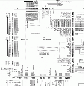
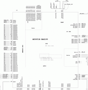
The golden data trove is here – http://www.readerme.com/html/html/%E7%9B%B8%E5%85%B3%E4%BA%A7%E5%93%81%E5%8E%9F%E7%90%86%E5%9B%BE%EF%BC%8C%E8%B4%B4%E7%89%87%E5%9B%BE.html
According to Anyka (安凯 in Chinese) the 36xx chips are a series, so they should have similar functionality.
While I don’t have data sheets, or a BSP, I can read the PDF’s at least to get an idea of where things are laid out.
They do look similar, so probably only minor differences in functionality (probably the newer ones are cheaper?).
Again, hard to check, as Anyka datasheets appear to be hens teeth.
I may give them a call also, and see if they’ll be willing to give us some info about their products, but I’m not holding my breath on that one.
I’ve also poked around a bit in the firmware files using strings, and taking a look at headers, and have come up with some preliminary conclusions.
I’m guessing their SoC is ARM5 based, given what i have found (haven’t decompiled yet, but looks like that).
Some common strings in the firmware’s from start:
00000 06 00 00 EA FE FF FF EA
Googling “06 00 00 EA FE FF FF EA” comes up with some other people talking about firmware for pxa312 devices, which have exactly that in their boot loader, so, seems likely.
The PXA312 is ARMv5TE…
I’m guessing some playing around with radare (http://radare.nopcode.org/get/radare.pdf.html) should get some more info about whats going on.
Running strings on the firmware files available shows interesting info:
strings /Documents/Keychain\ Camera/cx311V2.04/Spiboot_36XX.bin
ANYKA362
6KA49
start read cfg
file cnt:%d
file name:%s
Cannot find BIOS
read file info fail
load bios ……
map:%d
file len:%d
ld addr:0x%x
Load bios from spiflash successfuly!
read BIOS fail
spi boot start
system clock: %d
BIOS
Thats our 4k bootloader, which obviously loads our 1M bios image from SPI flash memory (SPI = Serial Peripheral Interface)
More on SPI here.
http://en.wikipedia.org/wiki/Serial_Peripheral_Interface_Bus
Hmm, more reasons for me to get a Bus Pirate now…
We have a flasher also, although its Windows based.
I’m guessing some USB sniffing will lead to some magic byte handshake sequence to get into the bootloader via USB, as the BIOS strings point to that.
eg:
“The setup packet is not 8 byte!”
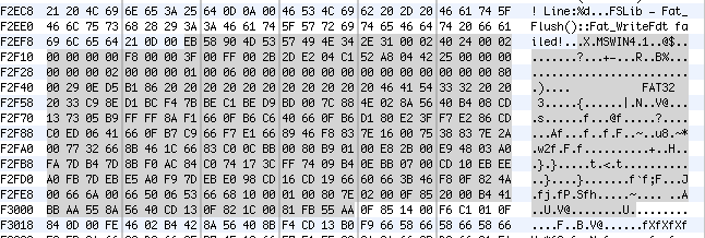
Also amusing is that its fairly easy to find the FAT32 code embedded in at least one of the firmwares
EB xx 90 … -> 55 AA (in Sprint1M.bin)
The flasher tool is also nice enough to give us an idea of layout in the 1M flash chip.
You’ll need to install the Anyka M3 USB driver to talk to the chip, which appears to have the following attributes via USB:
Vendor ID: 0471
Product ID: 0666 (the product of the beast? hehe)
This is a bit naughty, as 0471 is in theory already taken by Philips (or NXP) according to http://www.linux-usb.org/usb.ids
Its also astoundingly obvious that they used driverworks to make the driver. (From the oh so copied in China vid/pid, and the strings left in the driver). An example of this here http://www.baiheee.com/OpenSource/Easy%20USB%2051%20Programer/Easy%20USB%2051%20Programer_DriveOurBoard.htm
Want to bet someone read those instructions and its been repeated ad nauseum?
Sadly, its so easy to see the minimal effort that’s gone into things.
Back to our flasher, it says that our 1M chip is laid out as follows:
###Project Name
project name = chaoxian###Devie Number
device channel = 8###COM
com bOpen = 0
com base = 1
com count = 1
com baud rate = 38400path producer sundance2 = producer_sundance2.bin
path producer sundance2A uboot = producer_sundance2A_uboot.bin
path producer sundance2A umass = producer_sundance2A_umass.bin
path nandboot sundance2= Spiboot_36XX.bin
path nandboot sundance2A= Spiboot_36XX.binbios run addr = 0x30500000
bios start addr = 0xc0000
bios end addr = 0x1c0000
bios backup start addr = 0x1c0000
bios backup end addr = 0x2c0000chip type = AK_3225
chip uboot = 1
chip power off gpio = 255
chip usb2 = 0
chip get aid = 0
chip update = 0
chip select loop = 1
chip select nand0 = 1
chip select nand1 = 1
chip select nand2 = 1
chip select nand3 = 1
chip gpio_ce2 = 255
chip gpio_ce3 = 255ram size = 8
ram row = 12
ram column = 8
ram bank = 4moduleburn DownloadMode = 2
moduleburn bDownloadFLS = 1
moduleburn bDownloadEEP = 1
moduleburn baudrate = 921600
moduleburn gpio_dtr = 85
moduleburn gpio_module_igt = 109
moduleburn gpio_module_reset = 87
moduleburn path_fls = LCG2.fls
moduleburn path_eep = LCG2.eepfs start addr = 0x6c0000
fs reserver block = 64
fs nonfs reserve size = 4partition count = 0
download_to_udisk count = 0
download_to_nand count = 3
download_to_nand1 = 0, Spring1M_bios.bin, 0x30500000, BIOS
download_to_nand2 = 0, Spring.bin, 0x30000000, MMI
download_to_nand3 = 0, AkResData.Bin, 0x0, RESdownload_to_mtd count = 0
nand supported count = 0
If we take a look at that, our Spring1M_bios.bin starts off at C000
(bios start addr = 0xc0000)
(Deduct a 0 as we’re not offset by 0x300000000)
A look in a hex editor at that position shows:
Note the 32bit word value – 0xE1A0C00D
Thats classic ARM, so we _know_ its arm based…
romStart [0xe1a0c00d] mov r12,r13
Our next line of code is exactly the same as listed here http://code.google.com/p/milestone-overclock/wiki/Disassembly
e1a0c00d mov ip, sp
e92dd8f0 push {r4, r5, r6, r7, fp, ip, lr, pc}
So its looking like we can basically disassemble the code using arm-none-linux-gnueabi-objdump
I’ll leave that for another day, but with a bit more work we could compile our own code for this as we now have a good idea of the target cpu.
The next step would be to get into the bootloader or debug mode via USB, and see what can be seen.
Tools used:
0xED – http://www.suavetech.com/0xed/0xed.html
A nice fast and compact hex viewer for OSX.
strings – built into most *nix based systems.
Grey matter – Available to all, unused by many 😉
Now hopefully I can get back to the Webcam firmware stuff as I’ve been promising to do.
Archives
- November 2024
- November 2019
- October 2019
- August 2019
- April 2019
- February 2017
- September 2016
- June 2016
- May 2016
- September 2015
- August 2015
- June 2015
- April 2015
- December 2014
- October 2014
- September 2014
- July 2014
- June 2014
- April 2014
- October 2013
- July 2013
- May 2013
- April 2013
- March 2013
- January 2013
- December 2012
- October 2012
- August 2012
- July 2012
- June 2012
- May 2012
- April 2012
- March 2012
- December 2011
- November 2011
- October 2011
- September 2011
- July 2011
- May 2011
- April 2011
- March 2011
- February 2011
- January 2011
- December 2010
- November 2010
- October 2010
- September 2010
- August 2010
- July 2010
- June 2010
- May 2010
- April 2010
- March 2010
- February 2010
- January 2010
- December 2009
- November 2009
- October 2009
- May 2009
- April 2009
- March 2009
- February 2009
- January 2009
- December 2008
- November 2008
- October 2008
- September 2008
Categories
- Apple
- Arcade Machines
- Badges
- BMW
- China Related
- Cool Hunting
- Exploits
- Firmware
- Food
- General Talk
- government
- IP Cam
- iPhone
- Lasers
- legislation
- MODx
- MySQL
- notice
- qmail
- requirements
- Reviews
- Service Issues
- Tao Bao
- Technical Mumbo Jumbo
- Things that will get me censored
- Travel
- Uncategorized
- Useful Info
